
TL;DR:
- Nagoya University researchers have successfully predicted crystal orientation using AI and optical photographs of polycrystalline materials.
- Polycrystals, found in various industrial materials, have complex properties dependent on grain orientation.
- The AI model significantly reduces measurement time, taking only 1.5 hours compared to the traditional 14 hours.
- Large-area materials can now be measured, which was previously impractical.
- The technique offers the potential for revolutionizing materials development in industries reliant on polycrystalline materials.
Main AI News:
A groundbreaking research initiative led by Nagoya University scientists in Japan has achieved remarkable success in predicting crystal orientation through the utilization of artificial intelligence (AI) and optical photographs of polycrystalline materials. The team’s remarkable findings have been published in APL Machine Learning, catapulting their innovative approach into the spotlight of scientific advancement.
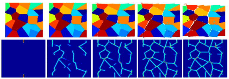
Crystals play a fundamental role in the functioning of numerous machines, with polycrystalline components frequently employed in a wide array of industries. Metal alloys, ceramics, and semiconductors are just a few examples of materials reliant on polycrystals. Due to their complex microstructure, consisting of multiple crystals, the orientation of crystal grains becomes a crucial determinant of their properties. This holds particular significance for silicon crystals, which are extensively used in the production of solar cells, smartphones, and computers.
“To attain polycrystalline materials suitable for industrial applications, precise control and measurement of grain orientation distribution are imperative,” remarked Professor Noritaka Usami. “Nevertheless, the high cost of equipment and time-consuming nature of existing techniques pose significant obstacles when it comes to assessing large-area samples.”
To overcome these challenges, the Nagoya University team, led by Professor Usami from the Graduate School of Engineering and Professor Hiroaki Kudo from the Graduate School of Informatics, joined forces with RIKEN to develop a machine learning model. This cutting-edge model analyzes optical photographs taken from various angles, effectively illuminating the surface of polycrystalline silicon materials. Remarkably, the AI-powered system successfully predicts the distribution of grain orientation.
“The entire process, from optical photography and training the machine learning model to predicting the orientation, takes a mere 1.5 hours,” explained Usami, highlighting the efficiency gains of their approach. “This stands in stark contrast to the traditional techniques, which demand approximately 14 hours. Moreover, our method allows for the measurement of large-area materials, an unattainable feat with conventional methods.”
Usami holds great optimism regarding the integration of their technique into industrial settings. “This technology possesses the potential to revolutionize materials development,” he stated with conviction. “Our research caters to researchers and engineers involved in the advancement of polycrystalline materials. By combining image data collection and a crystal orientation prediction model grounded in machine learning, it becomes conceivable to establish an orientation analysis system for polycrystalline materials. We anticipate widespread adoption of such equipment by numerous companies engaged in the production of polycrystalline materials.“
Conclusion:
The successful implementation of AI-based crystal orientation prediction has far-reaching implications for the market. By significantly reducing measurement time and enabling the assessment of large-area materials, this innovative technique addresses major challenges faced by industries utilizing polycrystalline materials. The improved efficiency and accuracy provided by AI-driven predictions will streamline manufacturing processes, leading to enhanced productivity and cost savings. Additionally, the prospect of an orientation analysis system based on machine learning opens up new avenues for materials development and innovation, promising a transformative impact on the market. Businesses operating in sectors such as electronics, solar energy, and semiconductor production should closely monitor these advancements to stay ahead of the competition and leverage the benefits of this groundbreaking technology.