
TL;DR:
- The research paper explores the transformative potential of generative AI in semiconductor design.
- Semiconductor design is highly complex, akin to planning a metropolis, involving numerous specialized teams and intricate processes.
- NVIDIA’s custom LLM, ChipNeMo, is a game-changer, trained on internal data to generate and optimize software, enhancing productivity.
- Three key use cases include a chatbot, code generator, and bug description automation, with promising results.
- The paper details the process of customizing LLMs, emphasizing the importance of data quality and staying updated on tools.
- NVIDIA Research is at the forefront of AI-driven innovations in the semiconductor industry.
Main AI News:
In the ever-evolving landscape of semiconductor design, where the complexity of crafting cutting-edge chips rivals that of planning a metropolis, a groundbreaking innovation is on the horizon. Today, we delve into the realm of generative AI and its profound impact on the semiconductor industry. This research paper not only sheds light on the possibilities but also demonstrates how it’s already transforming the way companies approach semiconductor design.
Semiconductor design is a formidable challenge, with chips resembling meticulously planned metropolises, housing tens of billions of transistors interconnected on pathways thinner than a human hair. This intricate orchestration involves multiple engineering teams collaborating for years to bring these digital megacities to life. Each team specializes in a distinct aspect of the process, from architectural blueprints to ultra-small circuitry and exhaustive testing, relying on specialized methods, software, and languages.
Mark Ren, an NVIDIA Research director and lead author of the paper, envisions a future where large language models (LLMs) become indispensable across all phases of semiconductor design. Bill Dally, NVIDIA’s chief scientist, echoed this sentiment during a keynote at the International Conference on Computer-Aided Design. He emphasized the significance of this pioneering effort, marking the initial strides in applying LLMs to the intricate domain of semiconductor design.
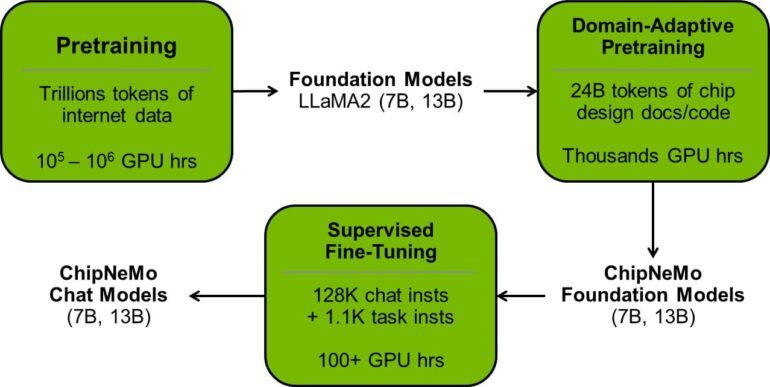
In this journey of innovation, NVIDIA engineers introduced a custom LLM, dubbed ChipNeMo, meticulously trained on the company’s internal data. ChipNeMo takes center stage in generating and optimizing software while providing invaluable assistance to human designers. The long-term goal is to harness generative AI at every stage of chip design, promising substantial boosts in overall productivity.
Three core use cases were identified to kickstart this transformation: a chatbot, a code generator, and an analysis tool. Among these, the tool automating the arduous task of maintaining updated bug descriptions garnered widespread acclaim. A prototype chatbot, designed to respond to queries related to GPU architecture and design, streamlined access to technical documents. Meanwhile, an evolving code generator has the capacity to produce software snippets in specialized chip design languages, seamlessly integrating with existing tools.
The paper primarily focuses on the meticulous process of gathering design data and employing it to craft a specialized generative AI model—a process adaptable to various industries. The foundation model chosen by the team was fine-tuned using NVIDIA NeMo, an integral component of the NVIDIA AI Enterprise software platform, boasting a staggering 43 billion parameters, indicating its prowess in pattern recognition. With training data encompassing over a trillion tokens, the model underwent refinement in two training rounds, utilizing extensive internal design data and a mix of conversation and design examples.
This pioneering work is just one example of the burgeoning role of generative AI in the semiconductor industry, emerging from the confines of research laboratories. One valuable lesson gleaned from this endeavor is the immense value of customizing LLMs. ChipNeMo, with as few as 13 billion parameters, demonstrated performance that rivaled or even surpassed much larger general-purpose LLMs, such as LLaMA2 with 70 billion parameters, in specific use cases.
As this transformative journey unfolds, it’s imperative for users to exercise caution in data collection and cleaning processes. Staying abreast of the latest tools capable of expediting and simplifying the work is equally crucial.
NVIDIA Research, with its global cadre of scientists and engineers, is spearheading innovations in AI, computer graphics, computer vision, self-driving cars, and robotics. Their foray into semiconductors encompasses AI-driven circuit design and optimized block placement, promising to reshape the industry.
For enterprises seeking to embark on their journey with custom LLMs, the NeMo framework, available on GitHub and NVIDIA NGC catalog, provides a promising starting point. In a rapidly evolving field, the era of generative AI in semiconductor design has arrived, heralding a new era of innovation and productivity.
Conclusion:
The integration of generative AI, exemplified by NVIDIA’s ChipNeMo, marks a pivotal moment in the semiconductor industry. This innovation promises to streamline and enhance the semiconductor design process, offering unparalleled opportunities for increased productivity and efficiency. As the industry continues to embrace generative AI, we can expect a significant transformation, ultimately leading to more advanced and efficient semiconductor products in the market.