
TL;DR:
- Advanced semiconductor packaging technologies like 2.5D and 3D hybrid bonding, alongside emerging solutions like silicon photonics, are driving innovation in AI and HPC chips.
- IDTechEx’s report analyzes trends, challenges, and market forecasts in semiconductor packaging, particularly focusing on 2.5D and 3D hybrid bonding.
- Large language models (LLMs) pose computational challenges due to their massive size and demand for high memory bandwidth.
- Industry initiatives aim to bridge the “memory wall” gap between processor compute density and memory bandwidth through innovations like NVLink, Infinity Fabric technology, and High Bandwidth Memories (HBMs).
- Increasing on-chip SRAM capacity and advancing semiconductor packaging technologies offer promising avenues to enhance system bandwidth and performance.
- Co-packaged optics emerges as a frontier, leveraging optical communication for superior bandwidth and data-intensive applications.
Main AI News:
In the realm of advanced semiconductor packaging, technologies such as 2.5D and 3D hybrid bonding, alongside emerging solutions like silicon photonics, are proving pivotal in optimizing system performance, heralding the next wave of innovation in AI and HPC chips. IDTechEx’s latest report, “Advanced Semiconductor Packaging 2024-2034: Forecasts, Technologies, Applications,” meticulously examines this evolving landscape, with a particular emphasis on 2.5D and 3D hybrid bonding packaging, while offering insights into technology trends, industry challenges, and the strides made by key players. Furthermore, the report forecasts market trends within the semiconductor packaging sector.
Embracing the Challenges of Large Language Models (LLMs)
The ascent of large language models (LLMs) stands as a significant milestone in artificial intelligence, fundamentally reshaping natural language processing (NLP) and its related domains. Models like OpenAI’s GPT series have showcased remarkable accuracy in comprehending, generating, and translating human language, thereby finding widespread applications across diverse fields. However, alongside their utility, LLMs also present formidable challenges.
The exponential growth in the size of LLMs, exemplified by the forthcoming GPT-4 boasting a staggering 1.76 trillion parameters, underscores the escalating computational complexity inherent in these models. For instance, GPT-4 demands over 1010 petaFLOPS for its operations. In comparison to conventional neural networks, LLMs necessitate significantly greater computational resources; the training of GPT-3, for instance, requires 3841 GPU hours as opposed to a mere 11 hours for a ResNet-60, a convolutional neural network employed in image classification tasks. Moreover, LLMs exhibit low operational intensity, heavily relying on matrix-vector operations, thus amplifying the importance of memory bandwidth in ensuring their optimal performance.
Enhancing System Bandwidth: Navigating the Memory Wall
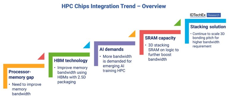
Recent years have witnessed a pronounced disjunction between the rapid escalation in processor compute density and the comparatively sluggish growth in memory bandwidth, giving rise to the ubiquitous “memory wall” conundrum. This disparity frequently results in processors idling as they await data, culminating in underutilization and posing a formidable obstacle to future performance enhancements.
To tackle this challenge, industry leaders such as NVIDIA and AMD have introduced innovative interconnectivity solutions like NVLink and Infinity Fabric technology, respectively, aimed at augmenting the bandwidth between CPU and GPU cores, thereby fostering enhanced system performance.
Furthermore, the integration of next-generation High Bandwidth Memories (HBMs) into architectures presents a promising avenue for bolstering logic-to-memory bandwidth. Traditionally confined to GPUs, HBMs are now making inroads into CPU designs, effectively bridging the bandwidth chasm between CPUs and conventional DRAM. AMD’s Instinct MI300 stands as a testament to this trend, seamlessly integrating advanced HBMs with both CPU and GPU components within a single package.
Moreover, 2.5D semiconductor packaging technologies, typified by TSMC’s Chip on Wafer on Substrate (CoWoS), play a pivotal role in amplifying the number of I/O points while concurrently reducing interconnect length between logic and memory components, thereby engendering heightened performance and diminished latency. However, the burgeoning demands of emerging HPC workloads, particularly those associated with AI training, necessitate even greater memory bandwidth, underscoring the imperative for innovation in this domain.
In response, novel processor designs have pivoted towards augmenting on-chip SRAM capacity, capitalizing on its proximity to processing chips to realize heightened bandwidth, denser interconnects, and reduced latency. Initial implementations leveraging 3D hybrid bonding packaging technology have demonstrated the efficacy of this approach, with the bonding of an SRAM die over a logic die at a 9 μm pitch resulting in a threefold increase in SRAM capacity. Subsequent refinements, characterized by a progressive reduction in the hybrid bonding pitch to 0.4 μm, promise to yield a substantial over 300-fold increase in bandwidth density, thereby charting a path towards enhanced system performance.
Embracing the Potential of Co-Packaged Optics
Amidst this backdrop, co-packaged optics emerge as a compelling frontier in system design, gaining significant traction in recent years. Leveraging optical communication confers several advantages over traditional electrical signal transmission, including reduced transmission loss, heightened resistance to crosstalk, and superior bandwidth capabilities, thus rendering it particularly well-suited for data-intensive applications.
In essence, the pursuit of high logic-to-logic and logic-to-memory bandwidth stands as a cornerstone of next-generation AI compute systems. Advanced semiconductor packaging technologies such as 2.5D and 3D hybrid bonding, coupled with emerging solutions like optical communication, are poised to play a pivotal role in facilitating this evolution, heralding a new era of computational prowess and innovation.
Unlocking Insights into the Future of Semiconductor Packaging
IDTechEx’s comprehensive report, “Advanced Semiconductor Packaging 2024-2034: Forecasts, Technologies, Applications,” offers a nuanced exploration of the dynamic terrain of 2.5D and 3D packaging, delving into technology trends, industry impediments, key player strategies, and market projections. Beyond elucidating the implications for AI and HPC applications, the report offers invaluable insights into sectors spanning 5G/6G, autonomous vehicles, and consumer electronics, providing stakeholders with a holistic understanding of how advanced packaging will shape the trajectory of these industries. With its impartial analysis and meticulous market assessments, this report stands as essential reading for stakeholders navigating the ever-evolving semiconductor landscape.
Conclusion:
The evolving landscape of advanced semiconductor packaging presents both challenges and opportunities for the market. Innovations in packaging technologies and interconnectivity solutions are essential for meeting the demands of AI, HPC, and other data-intensive applications. Stakeholders must leverage these advancements to enhance system performance and drive innovation across diverse industries.