TL;DR:
- NVIDIA unveils the H200 AI accelerator, boasting double the data processing speed and capacity of its predecessor.
- High Bandwidth Memory (HBM) technology is a key highlight, benefiting memory semiconductor companies like Samsung Electronics and SK hynix.
- H200 poses a direct challenge to AMD’s MI300X, emphasizing superior memory density and bandwidth.
- Global AI giants, including Amazon Web Services, Microsoft, and Google, are expected to leverage H200 for enhanced services.
- The launch intensifies competition in the high-capacity AI accelerator market, offering growth opportunities for memory semiconductor manufacturers.
Main AI News:
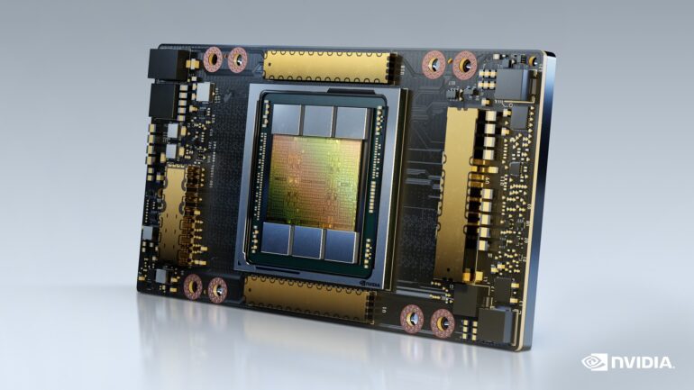
NVIDIA, a leading American fabless semiconductor company, has unveiled its latest Artificial Intelligence (AI) accelerator, the “H200.” The H200 is making waves with its impressive performance, boasting approximately double the data processing speed and capacity compared to its predecessor. What sets it apart is the extensive utilization of the 5th generation High Bandwidth Memory (HBM), pointing towards a significant boon for memory semiconductor companies such as Samsung Electronics and SK hynix.
The official announcement of the new AI accelerator, the H200, came on November 13th, local time. AI accelerators are semiconductor marvels crafted specifically for large-scale data learning and inference tasks, amalgamating Graphics Processing Units (GPUs), Central Processing Units (CPUs), HBM, and various other crucial components.
The H200 represents a substantial upgrade over its predecessor, the H100, which witnessed global demand, particularly for applications like training OpenAI’s cutting-edge large language model (LLM), GPT-4. Currently, a single H100 chip commands an estimated price range of US$25,000 to US$40,000, and it is known that thousands of these chips are required to power an LLM. While NVIDIA has not disclosed the exact pricing for the H200, servers equipped with this powerhouse are slated for an official launch in the second quarter of the coming year.
In its H200 unveiling, NVIDIA has emphasized the pivotal role of memory semiconductor technology. The H200 leverages the latest HBM3E, a 5th-generation HBM innovation. HBM is a memory semiconductor that maximizes data processing capacity and speed through vertical stacking of DRAM.
Thanks to HBM3E, the H200 achieves an astounding data processing speed of 4.8 terabytes (TB) per second and boasts a memory capacity of 141 gigabytes (GB). An NVIDIA representative elucidated, “When compared to the A100, a model from two generations ago, the H200 offers nearly double the capacity and 2.4 times more bandwidth.”
The launch of NVIDIA’s H200 is being seen as a direct challenge to its formidable competitor, AMD. Back in June, AMD introduced its latest MI300X, with the official launch scheduled for the next month. During the MI300X unveiling, AMD prominently highlighted its “2.4 times the memory density and 1.6 times the bandwidth compared to NVIDIA’s H100.”
Global AI giants like Amazon Web Services, Microsoft, and Google are poised to harness the capabilities of the H200 to enhance their service offerings.
Conclusion:
The introduction of NVIDIA’s H200 AI accelerator, with its superior performance and focus on High Bandwidth Memory technology, signals a heightened competition in the market. Memory semiconductor leaders like Samsung Electronics and SK hynix are positioned to benefit from this surge in demand, while global AI industry players stand to enhance their services. This development underscores the significance of memory semiconductor technology in the AI accelerator landscape and signifies growth prospects for the market.

