
TL;DR:
- Researchers at Nagoya University employ artificial intelligence (AI) to uncover the secrets of dislocations in polycrystalline materials.
- Polycrystalline materials, integral to modern technology, are complex and often prone to defects that affect performance.
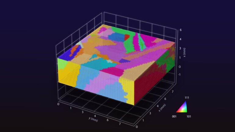
- AI technology constructs a 3D model to identify dislocation clusters in polycrystalline silicon, shedding light on their formation.
- Electron microscopy and theoretical calculations reveal stress distribution and unique nanostructures linked to dislocations.
- The discovery challenges the traditional Haasen-Alexander-Sumino (HAS) model’s understanding of dislocations.
- Unexpectedly, large tensile bond strains are found to trigger dislocation generation along the edges of specific structures.
- The breakthrough opens the door to universal guidelines for high-performance materials, with applications spanning from solar cells to semiconductors.
Main AI News:
In the realm of modern technology, the prevalence of polycrystalline materials cannot be overstated. From the sleek smartphones we carry to the robust metals and ceramics powering our automobiles, these materials are integral components. However, their complex structures have long posed a challenge for optimal utilization. Besides composition, a polycrystalline material’s performance is intricately influenced by its complex microstructure, dislocations, and impurities.
The Achilles’ heel of polycrystals in industry lies in the formation of minute crystal defects caused by stress and temperature fluctuations, aptly named dislocations. These dislocations disrupt the orderly arrangement of atoms in the lattice, consequently impacting electrical conduction and overall efficiency. To mitigate the risk of device failure, a comprehensive comprehension of dislocation formation is imperative.
Nagoya University’s distinguished team, led by Professor Noritaka Usami and including luminaries such as Lecturer Tatsuya Yokoi and Associate Professor Hiroaki Kudo, leveraged cutting-edge artificial intelligence (AI) to analyze image data of polycrystalline silicon—a material extensively employed in solar panels. The AI constructed a precise 3D model in virtual space, illuminating the regions where dislocation clusters were detrimentally affecting the material’s performance.
Having pinpointed these dislocation clusters, the researchers employed electron microscopy and theoretical calculations to unravel their origins. Their investigation unveiled stress distribution within the crystal lattice, highlighting intriguing staircase-like structures at the interstices between crystal grains. Remarkably, these structures appeared to be catalysts for dislocation formation during crystal growth. “We unearthed a distinctive nanostructure within the crystals linked to dislocations in polycrystalline structures,” remarked Usami.
Beyond its practical implications, this groundbreaking study could also reshape our understanding of crystal growth and deformation. The Haasen-Alexander-Sumino (HAS) model, a cornerstone theoretical framework for comprehending dislocation behavior in materials, may now need revision, as the team believes it may have missed these newly discovered dislocations.
The surprises did not end there. Upon calculating the atomic arrangement within these structures, the researchers stumbled upon an unexpected revelation—an unusually large tensile bond strain along the periphery of the staircase-like structures was found to trigger dislocation generation.
Usami elucidated, “As seasoned experts who have devoted years to this field, we were both amazed and exhilarated to finally unearth tangible evidence of dislocation presence in these structures. This suggests that we can exercise control over dislocation cluster formation by managing the direction of boundary expansion.”
Usami continued, “By employing polycrystalline materials informatics, a fusion of experimental data, theoretical insights, and AI to scrutinize nanoscale regions within polycrystalline materials, we have achieved a milestone in our understanding of these complex materials—a feat previously deemed unattainable.”
Conclusion:
This groundbreaking research not only deepens our understanding of polycrystalline materials but also holds significant implications for various industries. The ability to control dislocation clusters and improve material performance has the potential to revolutionize markets ranging from solar energy to electronics, ceramics, and beyond. Companies that can leverage this knowledge stand to gain a competitive edge in delivering high-performance materials to meet the demands of a rapidly evolving market.